8085 Architecture
Intel 8085 Microprocessor Architecture
The 8085 architecture microprocessor was one the first 8 bit processor launched by Intel in year 1976. This was also one of the most commercially successful processor that is still powering many devices.
After the success of 8085 processor , the Intel also launched many processors with 16 bit , 32 bit and 64 bit architecture.
It is important for the students of computer science to first study the 8085 architecture . This will help you understand some important foundational concepts.
These microprocessor foundational concepts will help you easily learn more complex processor architecture in future.
In this article you will learn all the foundational concepts necessary to understand the Intel 8085 microprocessor architecture, its technical features and the functions of the various functional units inside the 8085 processor chip.
8085 Architecture Video Tutorial
8085 Architecture Overview
The 8085 microprocessor is an 8-bit microprocessor introduced by Intel in 1976. It was widely used in early personal computers, embedded systems, and other electronic devices. Here’s an overview of the architecture of the 8085 microprocessor:
- Data Bus and Address Bus:
- The 8085 has an 8-bit data bus and a 16-bit address bus. This means it can address up to 64 KB of memory.
- Registers:
- The 8085 has six general-purpose registers, each of which is 8 bits in size: B, C, D, E, H, and L.
- It also has two 16-bit registers: the stack pointer (SP) and the program counter (PC).
- Accumulator:
- The Accumulator (A) is a special-purpose register used for arithmetic and logical operations. It is also used as one of the operands for most arithmetic and logic instructions.
- Flags:
- The 8085 has five flags: Sign (S), Zero (Z), Auxiliary Carry (AC), Parity (P), and Carry (CY). These flags are used to indicate the status of operations performed by the processor.
- Instruction Set:
- The instruction set of the 8085 consists of around 74 instructions, including arithmetic, logical, data transfer, control transfer, and input/output instructions.
- Control Signals:
- The 8085 uses a set of control signals to coordinate the operations of the microprocessor. These signals include Read (RD), Write (WR), Memory/IO (M/IO), and various other control signals.
- Interrupts:
- The 8085 supports five interrupt signals: TRAP, RST 7.5, RST 6.5, RST 5.5, and INTR. These interrupts allow external devices to request the attention of the microprocessor.
- Clock:
- The 8085 requires an external clock signal to synchronize its operations. The frequency of the clock signal determines the speed of the microprocessor.
The architecture of the 8085 microprocessor is relatively simple compared to modern microprocessors but was groundbreaking at the time of its introduction. Its 8-bit data bus and 16-bit address bus, along with its versatile instruction set and support for interrupts, made it a popular choice for a wide range of applications in the late 1970s and early 1980s.
8085 Architecture
Table Of Contents

8085 Architecture
How Microprocessor ( CPU ) Works ?
Let us first start with understanding the basic function of the microprocessor ( CPU ) , its internal architecture and how processor works.
Each microprocessor internally consist of three basic units which include the memory unit ( MU ) , control unit ( CU ) and the arithmetic & logic unit ( ALU ).
The CPU memory unit consist of high speed memory areas called registers. The control unit controls all the system components by sending the control signals along the control bus.
The arithmetic & logic unit ( ALU ) of the CPU performs all the arithmetic and logical operations as directed by the program instructions.
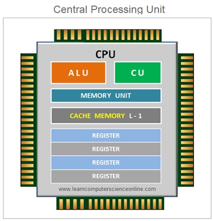
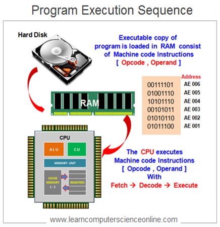
The main function of the microprocessor ( CPU ) is to execute the program. A computer program consist of set of instructions that directs the CPU to perform the desired operations.
The operating system loads the program into the main memory RAM . Each program instruction residing in the memory is a represented by machine instruction in binary.
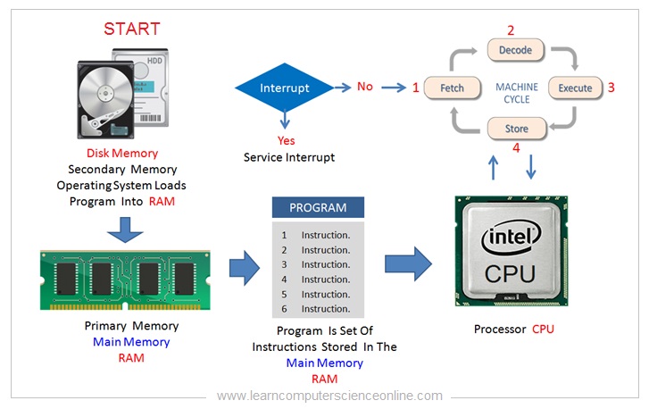
These machine instruction can be directly decoded and executed by the processor. The CPU initiates the program execution by fetching , decoding and executing each instruction one by one.
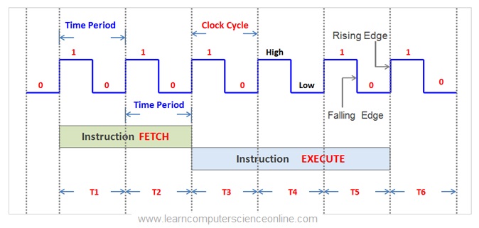
The CPU executes the program by repetitively performing the instruction cycle. The instruction cycle is a three step CPU operation which includes fetch , decode and execute operation.
8085 Architecture
Introduction To 8085 Processor
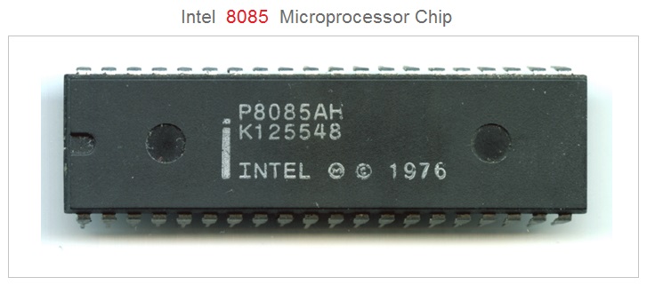
The Intel 8085 processor was launched as a successor to the Intel 8080 processor . The 8085 microprocessor is a 8 bit processor launched by Intel corporation in year 1976 .
The 8085 microprocessor was developed using the NMOS technology . The NMOS stands for negative channel metal oxide semiconductor which is a type of technology used to manufacture IC chips.
The 8085 processor is available in the market in many versions and used in many electronic gadgets such as washing machines , microwave ovens and other such devices.
8085 Architecture
What is Processor Architecture ?
The microprocessor architecture is defined as the layout and the description of its internal components. The efficiency and the performance of the processor depends upon its architecture.
The processor manufacturing companies such as Intel And AMD generally launch number of processor chips that belong to the same architecture family.
Each microprocessor family is characterized by its unique architecture . For example Intel Core i3 , Core i5 and AMD architecture family include Ryzen 3 , Ryzen 5.
The instruction set architecture ( ISA ) defines the set of binary commands supported by the processor and should not be confused with processor architecture.
8085 Architecture
8085 Architecture - Technical Features
Let us now understand the various technical features of the 8085 microprocessor architecture in detail .
- It is 8 Bit Processor
- It is a 40 Pin Processor.
- It works on +5 Volts Supply.
- Execution Speed - 3 , 5 , 6 MHz
- It has 8-Bit Data Bus ( 8 Bit Word Length).
- It has 16-Bit Address Bus.
- It can address up to 64 KB Memory.
- It has A 16-bit Program Counter Register ( PC ).
- It has A 16-bit Stack Pointer.
- It has six 8-Bit Registers : BC, DE, HL
- Supports 8 Software Interrupts .
- Supports 5 Hardware Interrupts .
The Intel 8085 microprocessor, introduced in 1976, is a popular 8-bit microprocessor that played a crucial role in the early development of personal computers and embedded systems. As a part of Intel’s 8080 microprocessor family, the 8085 offered improvements in terms of instruction set and capabilities.
8085 Architecture - Key Features
- 8-Bit Architecture: The 8085 is an 8-bit microprocessor, meaning it processes data in 8-bit chunks. This architecture influenced the design of early computing systems.
- Registers: It has six general-purpose registers, including B, C, D, E, H, and L, along with a 16-bit stack pointer and a 16-bit program counter.
- Clock Speed: The original 8085 microprocessor operated at a clock speed of 3 MHz, providing a reasonable balance between performance and power consumption.
- Instruction Set: The 8085 instruction set is well-defined and includes a variety of data manipulation, arithmetic, and control instructions. These instructions are encoded as 8-bit opcodes.
- Address Bus: The 8085 features a 16-bit address bus, allowing it to address up to 64 KB of memory. This capability influenced the memory organization of systems using the 8085.
- Data Bus: The data bus is 8 bits wide, allowing the microprocessor to transfer 8 bits of data between the microprocessor and memory or peripherals.
- Interrupts: The 8085 supports hardware interrupts, allowing external devices to interrupt normal program flow. This feature is crucial for real-time systems.
- Single Accumulator Architecture: Similar to its predecessor, the 8080, the 8085 uses a single accumulator architecture. The accumulator is a register used for arithmetic and logic operations.
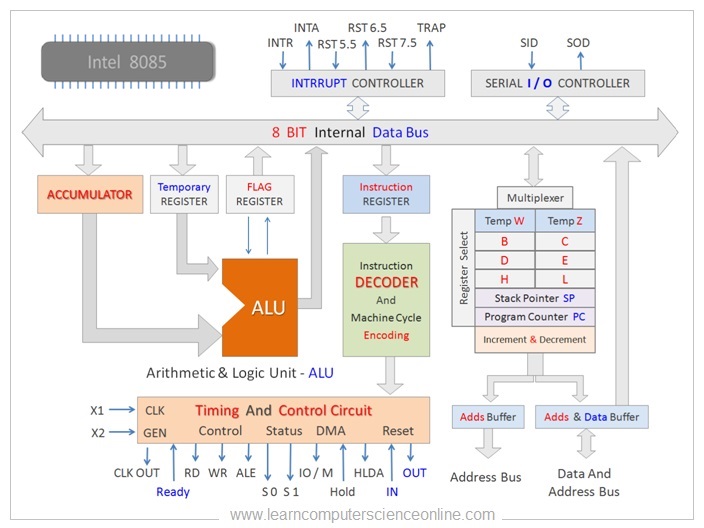
8085 Architecture - Functional Units
Like any other processor , the 8085 processor consist of number of functional units . Each functional unit performs a specific function during the program execution by the processor. These functional units are :
- Accumulator.
- Arithmetic And Logic Unit ( ALU ) .
- Timing And Control Unit.
- General Purpose Registers.
- Special Purpose Registers.
- Program Counter ( PC ).
- Stack Pointer ( SP ).
- Temporary Registers.
- Flag Registers.
- Instruction Register ( IR ).
- Instruction Decoder.
- Serial Input / Output Controller.
- Interrupt Controller.
- Address Bus And Data Bus.
8085 Architecture - Block Diagram

8085 Architecture
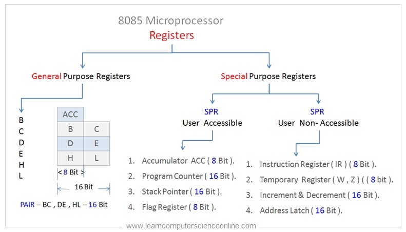
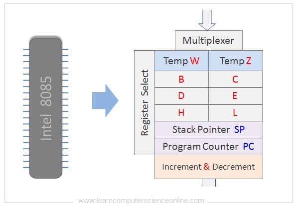
What Are CPU Registers ?
The CPU registers are simply high speed memory present inside the processor chip used by the CPU during the program execution. The CPU makes use of different types of registers placed inside the processor chip.
The CPU works at very high speed as compared to the speed at which the instructions and the data that can be fetched from the main memory RAM.
And therefore, the intermediate high speed memory is placed between the CPU and the main memory RAM in order to optimize the CPU performance.
Processor Registers Types
The CPU registers can be grouped into two types. The first type is called general purpose registers and the second type is called special purpose register.
The registers are groups of flip-flops used to store a word ( data ) . And each flip-flop can store one bit of data. For example if the word size is one byte then it will have eight flip-flops.
1. General Purpose Registers
2. Special Purpose Registers
A flip flop is an electronic circuit used to store two stable binary states that can be used to store the binary data either 0 or 1.
The programmer can directly access some registers by refereeing to their respective name and not by using their address.
8085 Architecture - Accumulator
The accumulator is a area where the processor actually operates on the data as per the operation code specified in the program instruction.
The accumulator is a type of 8 Bit register also referred to as ‘ACC’. The accumulator is connected to the internal data bus and the ALU.
The outcome of the operations carried out by the Arithmetic and Logical unit ( ALU ) is stored into the accumulator. The processed data is then transferred to the RAM.
Arithmetic And Logic Unit ( ALU )
The ALU is one of the most important functional component of the central processing unit ( CPU ). The main function of the ALU is to perform the arithmetic and logical operations.
The program instruction specifies the operation code ( OPCODE ) and the address of the data that needs to be fetched. The operation code is decoded and the ALU operates on the data placed in the accumulator.
The ALU performs various arithmetic operations such as addition , subtraction , multiplication , increment and decrement . The logical operations include decision making , comparison and other logical operations.
Timing Unit
8085 Processor Control Unit
The CPU is driven by a steam of clock signals generated by clock circuit within the processor chip. These clock signals helps the CPU to synchronize the operations of other hardware devices.
The control unit of the processor also sends control signals to all the hardware components and peripheral devices necessary to control its operations.
The timing and control signals are essential part of the instruction cycle which is a basic operation of the CPU to execute the program instruction. For each clock pulse the CPU executes a part of the instruction.
Read More
8085 Architecture
General Purpose Registers
The general purpose registers are used to data in the temporary memory during the program execution. The 8085 processor has six general purpose registers that can store 8-bit data.
The general purpose registers are named as B, C, D, E, H, and L. These registers can also be combined to form a register pair such as BC, DE, and HL, to perform 16-bit operations.
These registers are used as high speed temporary memory to store the program data during the program execution.
8085 Architecture
Special Purpose Registers
The CPU also make use of some special purpose registers during the execution of the instruction cycle .
These CPU register are used to store a specific type of data and assigned a special function and therefore they are called special purpose registers.
The general purpose registers are used to store any type of data ( address or instruction or other data ). Whereas the special purpose registers datatype and its purpose is predefined.
For example the program counter can only store address , the instruction register can store only instruction and the accumulator can store the data ( Operand ) that needs to be operated by the ALU.
Flag Register
What Is Flag Register In 8085 Architecture ?
The main function of the flag register is to indicate the status of the processor after the ALU operation. The flag register is also alternately referred to as program status word ( PSW ).
A flag register is a 8 bit special purpose register used in 8085 architecture to indicate the CPU status after each arithmetic and logical operation.
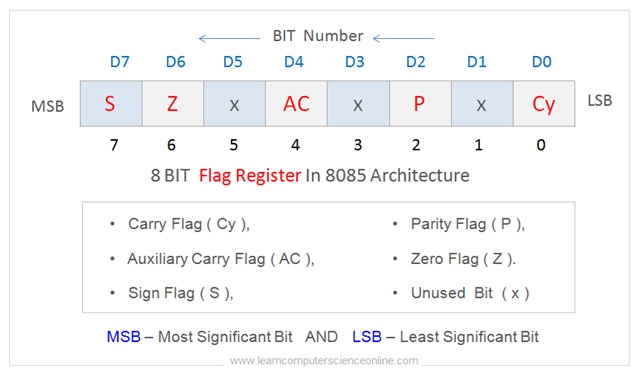
The 8085 flags register can have a total of eight flags. Each flag is represented by a specific bit in the 8 bit flag register.
Each flag is represented by a single bit. A flag can be either set to binary 0 or it can be reset of binary 1. In other words , a flag can either be 0 or 1.
In 8085 processor use only five flags and the remaining three flags are kept unused. The five flags used include :
Carry flag ( Cy ), Auxiliary carry flag ( AC ), Sign flag ( S ), Parity flag ( P ), and the Zero flag ( Z ).
Instruction Register
What Is Instruction Register In 8085 Architecture ?
The instruction register ( IR ) is a 8 bit special purpose register used by the processor to store the part of the instruction that is decoded by the control unit.
The instruction register is a non-accessible type of special purpose register and the programmer cannot directly modify its contents.
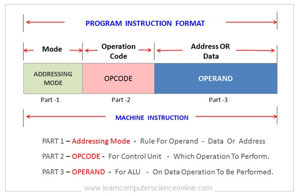
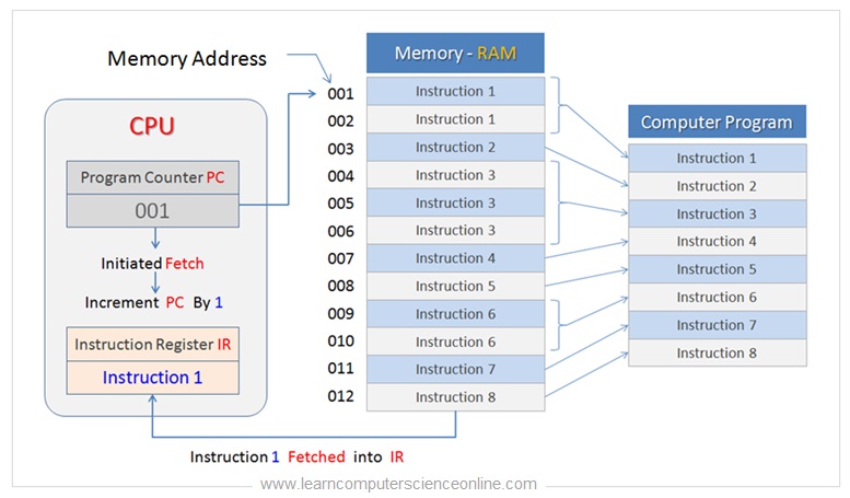
The CPU fetches the instruction from the main memory RAM. Depending upon the instruction format , the control unit of the CPU decodes the instruction as specified in the OPCODE of the instruction format.
The OPCODE part of the instruction is stored into the 8 bit instruction register ( IR ) during the program execution ( Instruction Cycle ).
Program Counter ( PC )
What Is Program Counter In 8085 Architecture ?
The program counter ( PC ) is a 16-Bit special purpose register used in the 8085 architecture to store the instruction address.
The program counter register always stores the memory address of the next instruction that needs to be fetched from the main memory ( RAM ).
During the execution of the instruction cycle the PC is always incremented by one just after the fetch operation of the current instruction is initiated by the CPU so that it points to the next instruction to be fetched from the memory.
8085 Architecture Interrupts
The interrupts are the signals sent to the microprocessor to pause and attend the request sent by the external devices. In other words . the interrupts are external events that occur in real time to seek the processor response.
The interrupts can either be generated by the program instructions or it can also be generated by the peripheral devices connected to the system.
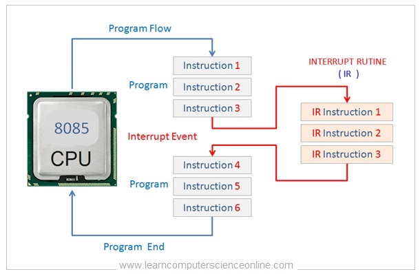
The 8085 architecture supports eight software interrupts and five hardware interrupts. The Interrupt can be classified into following groups depending upon their parameters :
8085 Architecture
Interrupt Types In 8085 Architecture
- Software Interrupt.
- Hardware Interrupt.
- Vector Interrupt.
- Non - Vector Interrupt.
- Maskable Interrupt .
- Non-Maskable Interrupt.
Software Interrupts
The software interrupts are generated during the program execution in response to the instruction.
These interrupts are specifically added into the program by the programmer while writing the program code.
The 8085 architecture supports 8 software interrupts. These software interrupts include RST0, RST1, RST2, RST3, RST4, RST5, RST6, and RST7.
Hardware Interrupts
The hardware interrupts are generated by the hardware peripheral devices connected to the system.
The 8085 architecture supports 5 hardware interrupts. There are 5 interrupt pins present in the 8085 chip used as hardware interrupts. These include TRAP, RST7.5, RST6.5, RST5.5, INTA.
Vector Interrupts
The vector interrupts have fixed vector address and the interrupt address is known to the processor. For example: RST7.5, RST6.5, RST5.5, TRAP.
Non-Vector Interrupts
The non-vector interrupts are interrupts when the interrupt address is not known to the processor .
For these interrupts the device address needs to be sent to the processor in order to service these interrupts. For example : INTR.
The device that generates an interrupt gives the address of interrupt sub-routine for these interrupts. The INTR is the only non-vectored interrupt in 8085 architecture.
Maskable Interrupts
The maskable are those interrupts that can be disabled by the programmer by writing some specific instructions into the program code.
The maskable interrupts can also be ignored by the processor. For example : RST 7.5, RST 6.5, and RST 5.5.
Non-Maskable Interrupts
The non-maskable interrupts cannot be disabled by the programmer by writing some specific instructions into the program code.
The non-maskable interrupts cannot be ignored by the processor and enjoys the highest priority. For example : TRAP.
8085 Architecture
Bus Interface In 8085 Architecture
The computer buses are the group of wires running across the computer system through which data , address , control signals are transferred.
The microprocessor needs to communicate with various system hardware components in order to execute the program instructions.
The microprocessor chip also has its own internal buses essential for the functioning of the processor. The 8085 architecture has 8 bit data bus and 16 bit address bus.
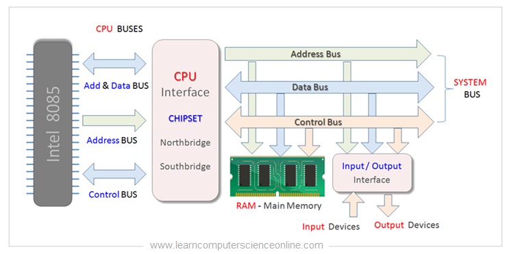
Address Bus
The address bus is a 16 bit unidirectional bus that is used to transfer the 16 bit address between the CPU and the main memory RAM.
During the CPU fetch operation , the address is transferred from program counter ( PC ) register to the memory controller on the 16 bit address bus.
Data Bus
The data bus is a 8 bit bidirectional bus that is used to transfer the 8 bit data between the CPU and the main memory RAM.
The CPU performs both memory READ and WRITE operation during the program execution . The data transfer takes place on the data bus.
Control Bus
The control bus is a bidirectional bus that is used to transfer the control signals between the CPU and the various hardware devices connected to the computer system.
8085 Architecture
Join The Best Seller
Computer Science Online Course
This is the most comprehensive and unique Computer Science And Programming Fundamentals course Online which will give you in depth understanding of most important fundamental concepts in computer science And Programming .